At PTC we don’t just have theoretical knowledge, we are hands on semiconductor assembly, packaging, test, and business development experts that can bring you factory solutions to life.
Contact Us


A Growing Need For Semiconductor Factories
162%
Estimated Semiconductor Industry Growth by 2029
56%
Demand For Manufacturing Capacity to Increase
53 billion
Invested by U.S. Government in Semiconductor Industry by 2030.
Global Investment
High Global Private & Government Investment in Emerging Semiconductor Markets such as India
“ Our goal at PTC is to develop and optimize the semiconductor ecosystem globally and especially in emerging tech markets. “
Raja Manickam, Founder
Factory & Business Services
Factory
Factory Layout and Environment Controls
Quality Assurance and Control Implementation
Equipment Procurement and Installation
Technology Transfer Planning
Package Design and Bill of Material Selection
Process Development and Optimization

Product and Process Qualification

Production Scaling & High-Volume Manufacturing Ramp
Factory Build–Operate–Transfer
Factory Certification
Supply Chain Development and Optimization
Workforce Setup and Training
Business

Semiconductor Product Ecosystem Consulting: Monetize, Manufacture, and Deliver

Risk Assessment and Risk Mitagation

Sales and Business Development Support

Government and Private Partnership Development

Factory Due Diligence and Auditing Services
Cost Models
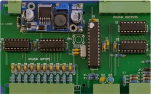
Industries & Applications Expertise
Our Consultants have supported various Industries and Applications including the ones below.

RF

Automotive

Solar
Micro-Controllers
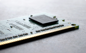
Memory
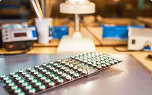
LED

Power
Sensor
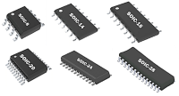
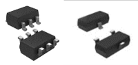
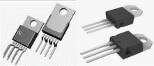
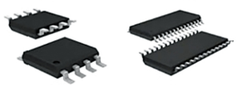
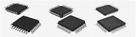
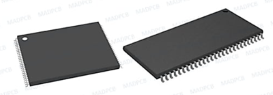
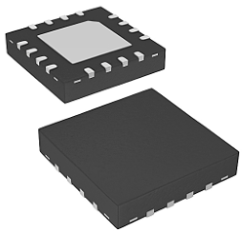
Roadmap of Packages Supported by Our Consultants
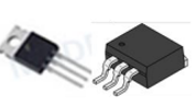
TO
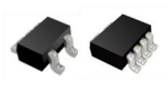
SOT
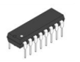
DIP
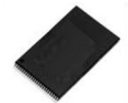
TSOP
PLCC
LQFP / TQFP
QFP
HSBGA
LBGA
PBGA
BGA Stack Die

Diode package for Solar application
Solar CPV Module

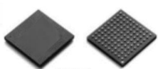
QFN Stack Die Flash die stack on IC

QFN

PQFN – Cu Clip Exposure Copper

FCBGA

SIP LGA

SIP- QFN
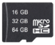
uSD

SD Card
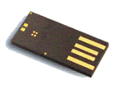
USB
Auto Front Lighting Micro-LED

Double Sided Molding
Wettable flank QFN

Smart Card
Package/Product Experience Examples
IC Package Legacy Product
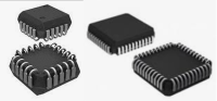
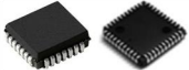
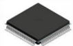
PLCC Families
SOIC Families
SOT Families
TO Families
SOP Families
QFP Families
TSOP Families
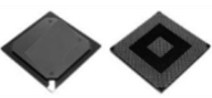
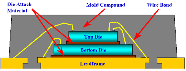
QFN module (stack Die)
-
-
- Typically having flash memory die (EEPROM) stacked on controller die.
- Options of multiple controller for increased functionality.
-
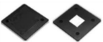
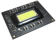
Power QFN Package
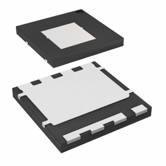
Single Cool

Dual Cool
-
-
- Power QFN combined with copper clip replaces the traditional wire bond interconnect for high performance MOSFETs by providing lower resistance and inductance than multiple wire bonds to improve thermal performance.
- Options of Single-Cool (embedded Cu clip) and Dual-Cool (expose Cu clip).
-
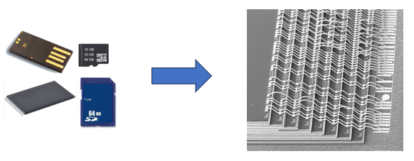
Memory Devices
-
-
- Different variance of memory packages : TSOP, micro-SD, SD Card and USB.
- Multiple stack NAND die with different technology with thickness up to 4 stack.
-
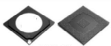
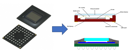
CMOS Image Sensor Product
-
-
- CMOS Image Sensor with different platform of CLCC (Ceramic) and iBGA (laminate substrate).
- Commonly used in automotive, unattended surveillance, stereo vision, security, smart vision, automation, and machine vision.
-
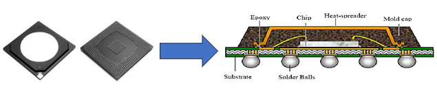
BGA with Expose Heat Spreader
-
-
- Heat spreader attached on top of punch BGA for improved thermal performance.
- Typically used on a device having high thermal conductivity that is used to move heat from a concentrated or high heat flux source to a heat exchanger with a larger cross section area, surface area, and volume.
-
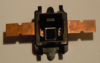
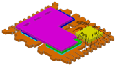
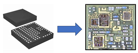
Power QFN/LGA/BGA Module with Thick Component (5mm thickness package)
-
-
- Controller IC die/package with typical passive component & large component such as an inductor.
- Substrate interposer to improve circuit routabality.
- Multiple copper wires and/or Al ribbon for power application.
- SIP integration to improve device functionality and performance.
-
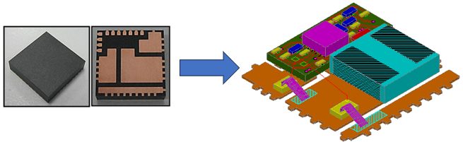
RF SIP LGA/ BGA Module with COB
-
-
- Multi die LGA module with passive component for QFN application.
- Key Features:
- Compact design
- Short wire length
- Cost efficient
-
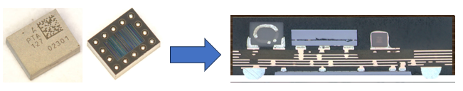
RF SIPLGA/ DSMBGA Module with SMT + MCOB
-
-
- Double Sided Molded Ball Grid Array (DSMBGA) package which allows molded assembly of components on both sides of the substrate.
- SIP module is a package that contains an electronic system or sub-system and is miniaturized through IC assembly.
-